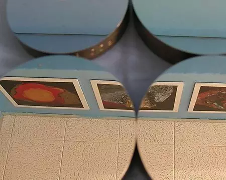
Polishing Precision Optics - Photonics and Optical Components Surface Finishing
What are Precision Optics
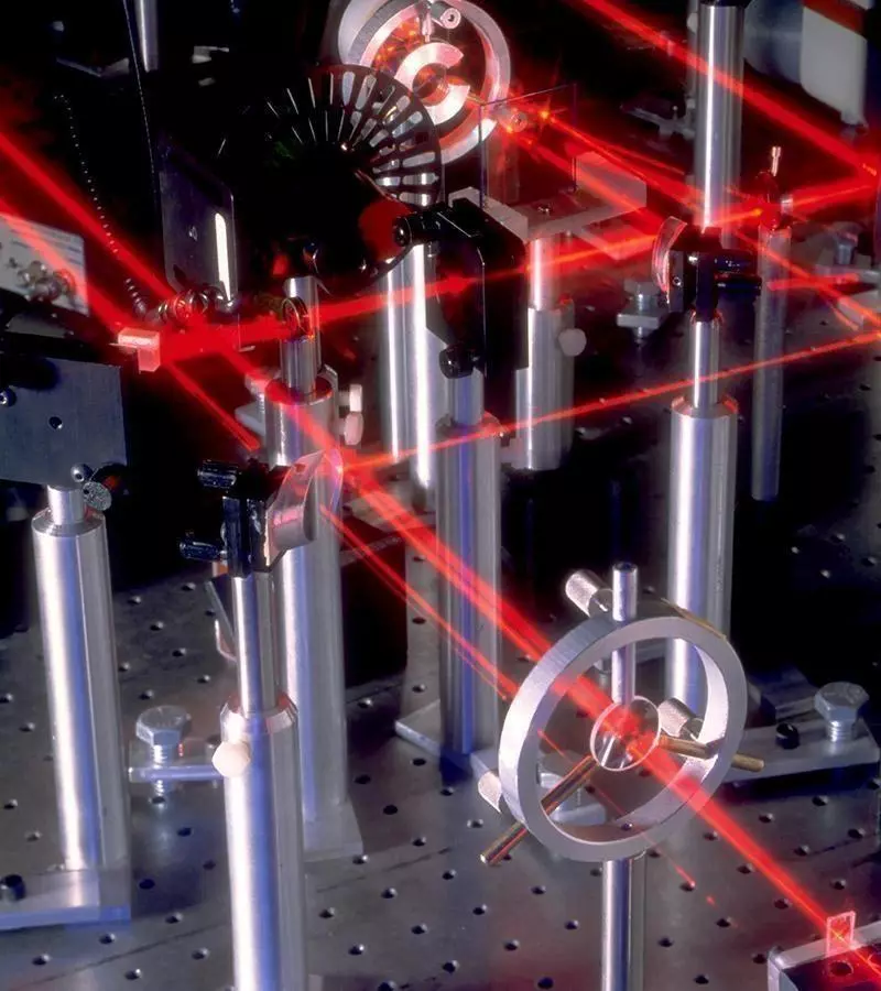
Precision Optics is the use of optical components and elements in electro-optic devices. These devices are used for the detection, sense, transmittance, and effects of light energy. It works with light energy of specific wavelengths and the changes in its spectrum. Multiple geometries and surfaces are being created to get optical properties according to requirements. These properties are dependent not only on the geometry of materials but also on the type of material used. It helps the manufacturers to acquire a required set of properties according to the need of the application. Specific designs are made to cater to the modern world's requirements. There are different types of precision optics applications including laser optics, infrared optics, achromatic optics, and optical prisms. It is the combination of glass and plastic optics to obtain a targeted set of properties. Precision optics has introduced a whole new concept of very small lead times and delivery times as well. Quick light signal processing has been achieved by using modern precision optics concepts. Miniature devices and machines are continuously developed using precision optics materials. Moreover, precision optics are useful for applications where you have to use light for precise measurement, structuring, analysis, and processing to a higher level of accuracy. Photonics Photonics is a technology that uses photons. Therefore, it deals with the study of photons generation, transmission, energy loss, modulation, signal generation and processing, amplification, switching, and sensing. Photonics is a modern field that is becoming popular for advanced optical devices. It considers the generation, transmission, control, and detection of photons. It works for the development of smart technology applications that are implemented in our daily lives.
What is Photonics Engineering
It is the branch of engineering that deals with the study of light energy and information to create advanced technology in multiple fields such as instruments for healthcare, construction, information technology, communication, etc. Almost every industry is requiring photonics engineers to make advances in the field. Replacement of conventional light transmittance procedures needs efficient photonics devices that are possible to be made by using expert engineering knowledge. It has helped the communication industry to move towards a better future with higher efficiency and low delivery times. Photonics engineering makes you capable of generating and studying nanostructured materials that can exceptionally perform well and be used in optical devices of the modern era. It also identifies the techniques, tests, and procedures with which optical structures are visualised, monitored, amended, and used. Multiple components are being developed for optoelectronic devices that add to the efficiency of electrical circuits.
Importance of Photonics
Photonics plays a major role in the development of modern technology including smart electronic devices, industrial-level machines, faster communication through fibre optics and the internet, reducing the size of devices, and making intricate structures with high efficiency. Principles of photonics are extensively used in different fields to create wonderful instruments. It is one of the major sources of innovation in industries that make use of optics. It generates new directions for material choice, processing, device fabrication, data storage and transmission, and many more. It offers a new way to overcome the limitations of storage, accuracy, and speed in conventional devices. It contributes to light-saving procedures that make processes sustainable in energy development. So, it is not only helping in cost-effectiveness but also saving the people and the environment. There are photonic sensors that are contactless and are used efficiently to detect any hazardous thing for humans. Photonics makes an efficient implementation of particulate properties of light for developing modern optoelectronic and photonic devices for telecommunication, laser, LEDs, and many more.
Difference between Optoelectronics and Photonics
Optoelectronics deal with light emitting devices or light detecting devices while photonics deal with the physical science of light and its applications. Optoelectronics is an electronics branch that is just specified for optical applications. Photonics is more towards optics study i.e., relating to physical properties and phenomena. Source of light, detection and control is studied under optoelectronics for diodes, transistors, and other optical components of electronic devices. Therefore, photonics mostly deals with the study of physics and relating it to the optical phenomenon of light. Optoelectronics is more towards the electrical implementation of a phenomenon that is studied in photonics. Both branches are interlinked for the development of optical devices for precise applications ranging from household applications to space technologies.
Surface Finishing of Optical Components
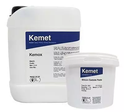
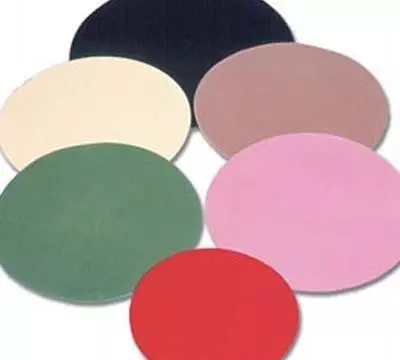
Surface finishing techniques are very crucial and specified depending on the type of material and its application. Rastering or rotating the optical components in a fluid is commonly used in surface finishing procedures. Surface properties are controlled by surface finishing processes. Roughness, atomic concentration, and related properties of optical components are optimised for optimal reflective, refractive, transmittance, and related properties. Polishing pads, ultra-polishing pads, contact polishing, and quasi-polishing pads are used for this purpose. The better the surface finishing technique used, the better will be the optical properties of the prepared material. Bowl feed polishing is a technique that is employed for the ultrasmooth surface of up to 0.3 nm RMS value. Bonnet polishing is also employed where the surface roughness of up to 80 nm is required in the optical components. If a further improved surface is required, slurry jet polishing is used. It can be seen that the surface finishing operations of optical components are more difficult and expensive as well due to the very precise needs of optical specifications. To view the structure of any optoelectronic components, it must be first cleaned efficiently for better visuals and image creation. Kemet offers excellent surface finishing processes for most optical components and materials, some of them are described below concerning their uses and surface finishing properties.
Beta Barium Borate
Beryllium Copper
Lapping & Polishing Beryllium Copper - Case Study
Test Requirements: Optical finish, no specific flatness required
Component/Material: Various Beryllium Copper samples
Stage 1
Machine Type: Kemet 15” diamond lapping/polishing machine
Lap Plate: Kemet XP
Abrasive Type/Grade: 3µ Type K STD Diamond slurry
Additional Pressure: 4 Kg
Stage 2
Machine Type: Kemet 15” diamond lapping/polishing machine
Lap Plate: ASFL-AW silk cloth
Abrasive Type/Grade: 3µ Type K STD Diamond slurry
Additional Pressure: 4 Kg
Stage 3
Machine Type: KemCol 15 - Chemical Mechanical Polishing Machine
Lap Plate: Chem Cloth
Abrasive Type/Grade: Col-K
Additional Pressure: 4 Kg
| Process Breakdown | ||||
|---|---|---|---|---|
| Stage | Plate/cloth type | Abrasive type/grade | Dispenser settings | Process time |
| 1 | Kemet XP | 3µ Type K STD Diamond slurries | 2 seconds spray every 30 seconds | 15 minutes |
| 2 | ASFL-AW silk cloth | 3µ Type K STD Diamond slurries | 2 seconds spray every 30 seconds | 5 minutes |
| 3 | Chem Cloth | Col-K CMP Slurry | Constant drip feed from peristaltic pump | 5 minutes |
Stage 1:
This is a grading stage to produce a good flat surface and finish. Initially we ran the component on a Kemet XP plate using a 3µ slurry with 4kgs weight for 15 minutes. This produced a good reflective finish with some scratches visible.
Stage 2:
This is a pre-polishing stage, which gives a good reflective finish and prepares the component for final polishing. The component was then run on an ASFL-AW silk cloth using a 3µ type K STD slurry for 5 minutes with 4kgs of weight to produce a 90% blemish free finish.
Stage 3:
Polishing stage, gives a blemish free mirror polish. Finally the component was run on a CHEM cloth using COL-K colloidal silica with 4kgs of weight for 5 minutes. This produced a blemish free mirror polish.
Recommended minimum equipment required to run 1 component
- 1 x Kemet 15” Diamond lapping machine or larger
- 1 x Kemet 15” Col-k Colloidal silicate lapping machine or larger
- 1 x Kemet XP plate
- 1 x Kemet Stainless Steel plate for Col-K
- 1 x ASFL-AW silk cloth
- 1 x Plastic faced control ring
- 3µ Type K STD diamond slurry
- Col-K Colloidal Silicate
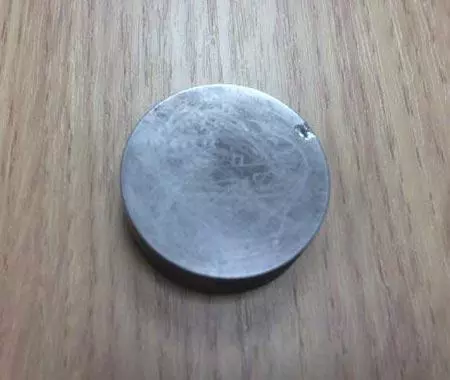
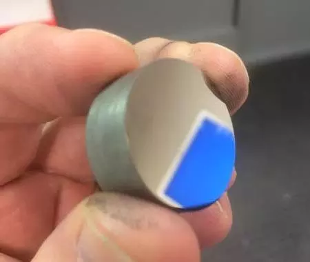
Before Polishing Beryllium Copper
After Polishing Beryllium Copper
Cadmium Sulfide
Calcium Fluoride
Fused Silica
Fused silica is the amorphous form of silicon dioxide that is used mainly in optical instruments like lenses, mirrors, metrology components, and parts of optoelectronic devices. As we know, there is a very high demand for the surface finish to aid the reflection, refraction, or transmittance of light. To fulfil this demand, abrasive powders have been used for surface finishing. Cerium oxide particles are used as abrasive powders. Moreover, Kemet has developed a polishing procedure that is very effective in obtaining a highly flat and pure fused silica surface.
Gallium Arsenide
Germanium
Lapping & Polishing Germanium Parts - Case Study
Test Requirements: To lap germanium discs with surface finish Ra<0.01 µm, Rz<0.05 µm;flatness < 1µm; parallel < 3 µm.
Component/Material: 6 x 25mm diameter Germanium
Stage 1
Machine Type: Kemet 15” diamond lapping/polishing machine
Lap Plate: Cast Iron
Abrasive Type/Grade: Kemox 0800S
Additional Pressure: 4 Kg
Stage 2
Machine Type: Kemet 15” diamond lapping/polishing machine
Lap Plate: ASFL polishing cloth
Abrasive Type/Grade: Kemet Liquid diamond Type K 1 Micron standard
Additional Pressure: 4 Kg
| Process Breakdown | |||
|---|---|---|---|
| Stage | Plate/cloth type | Abrasive type/grade | Process time |
| 1 Lap | Cast iron | Kemox 080S | 2 mins per side |
| 2 Pol | ASFL Polishing pad | Kemet Liquid diamond Type K 1 Micron | 5 Mins per side |
Comments:
Flatness required: < 3 µm . Preferably 1 µm
Flatness achieved: 2 light band = 0.67 µm
Ra required Ra: 0.01 µm
Ra achieved: 0.059 µm
Rz required: 0.05 µm
Rz achieved: 0.0253 µm
Before Lapping & Polishing Germanium
After Lapping & Polishing Germanium
Lithium Niobate
Lithium Triborate
Magnesium Fluoride
Quartz
Polishing Quartz - Case Study
Test Requirements: To lap and polish 2 samples of Quartz to flatness better than 1 um and Ra better than 1nm
Component/Material: 1 quartz glass tube (OD ~62mm) sample and 1 quartz glass rod (OD ~41mm)
Machine Type: Kemet 15” diamond lapping/polishing machine
| Process Breakdown | |||
|---|---|---|---|
| Stage | Plate/cloth type | Abrasive type/grade | Process time |
| 1 Lap | Cast iron | Kemox 0-800s | 2o minutes |
| 2 Pol | PSU-M Polishing pad | Kemox WC | 50 minutes |
The glass was held on the weights using a non-slip film.
Quartz sections were initially cut on Micracut 201 precision saw using diamond cut off wheel and a slow feed rate. This produced a clean cut with minimal chipping
After lapping & polishing, the middle of the part is flat to 1-2 light bands (< 1 micron).
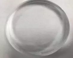
Before Polishing Quartz

After Polishing Quartz
PR3 Plate Quartz Polishing Test
Work Size: φ100mm×6mmT
Polishing Condition: In-Situ method. The benefit of using the dresser is that it keeps the cutting rate and maintains the PR3 plate flatness.
Plate: 15” PR3 Plate Conditioned by facing unit
rpm: 40rpm
Slurry: Cerium oxidie (Size 1~2µm 5%/wt)
Flow amount : 5ml /min
Process 1: Pressure 80g/cm2 30 min
Process 2: Pressure 30g/cm2 20 min
Flatness Result: 0.130µm(λ/4.88)
Sapphire
Silicon
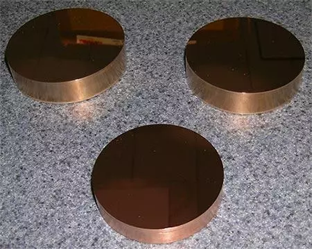
Silicon Carbide (SiC)
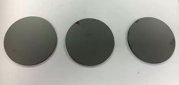
Polishing Silicon Carbide - Case Study
Test Requirements: To produce best surface finish on 65mmø Silicon Carbide blanks prior to pitch polishing.
Component/Material: Silicon Carbide blanks
Stage 1
Machine Type: Kemet 15 diamond lapping/polishing machine
Lap Plate: Kemet Iron with spiral grooves
Abrasive Type/Grade: Kemet Liquid Diamond Type K 14 Micron standard
Additional Pressure: 3.5Kgs for 1 part
Stage 2
Machine Type: Kemet 15 diamond lapping machine with facing unit
Lap Plate: Kemet Copper with spiral grooves
Abrasive Type/Grade: 6-KDS1488 (water-based)
Additional Pressure: 4 Kg
Stage 3
Machine Type: Kemet 15 diamond lapping machine with facing unit
Lap Plate: Pure Tin
Abrasive Type/Grade: 0.75-KDS1438 (water based)
Additional Pressure: 4 Kg
| Process Breakdown | ||||
|---|---|---|---|---|
| Stage | Plate/cloth type | Abrasive type/grade | Dispenser settings | Process time |
| 1 | Kemet Iron with spiral grooves | Kemet Liquid Diamond Type K 14 Micron standard | 2 second spray every 40 seconds | 5 - 10 minutes (Front Surface) |
| 2 | Kemet Copper with spiral grooves | 6-KDS1488 (water-based) diamond slurries | 2 second spray every 40 seconds | 10 - 15 minutes |
| 3 | Pure Tin | 0.75-KDS1438 (water based) diamond slurries | 2 second spray every 40 seconds | 1.5 - 2 hours |
Results:
Stage 1: - This process removed 10 - 20 µm in 5 - 10 minutes. The surface finish achieved ranged from 0.08 ~ 0.084µm.
Stage 2: - This pre-polish step gives a semi-reflective surface with surface finish of Ra 0.056 ~ 0.060µm.
Stage 3: - The polishing process results in a mirror surface finish of Ra 0.007µm.
After Stage 1 Polishing Silicon Carbide
Conclusion
In order to improve surface finish and flatness, pitch polishing should be used
Flatness was measured on a Zygo and was 0.341 µm (Peak to Valley)
Final Flatness After Polishing Silicon Carbide

Yttrium Aluminum Garnet (YAG)
Zinc Selenide
PR3 Polishing Plate For Optics
The Kemet PR3 Polishing Plate is a new alternative to using polyurethane pads for polishing precision optics. The plate consists of a thermally stable resin and can be used with cerium oxide, aluminium oxide and diamond slurries. Kemet PR3 can be supplied as complete plates in most diameters or as discs for fixing to your machine base plate.
- Excellent Flatness produced – below 0.08 micron
- Improved Edge Exclusion - No fall off at the edges.
- Produces excellent surface finishes down to 1nm
- Easy to machine.
- Ideal for polishing optical glass